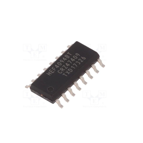
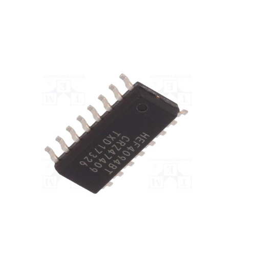
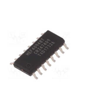
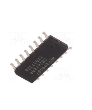
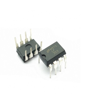
NXP HEF4094BT 8-Stage Shift and Store Register SMD
₹32.00
The HEF4094B NXP Semiconductor is a serial shift register with eight stages. Each stage has a storage latch for strobing data from the serial input to the parallel buffered 3-state outputs QP0 to QP7.
2 in stock
The HEF4094B NXP Semiconductor is a serial shift register with eight stages. Each stage has a storage latch for strobing data from the serial input to the parallel buffered 3-state outputs QP0 to QP7. The parallel outputs can be directly connected to common bus lines. On positive-going clock transitions, data is shifted. When the strobe (STR) input is HIGH, the data in each shift register stage is transferred to the storage register. When the output enable (OE) signal is HIGH, data from the storage register appears at the outputs. Two serial outputs (QS1 and QS2) are provided for cascading multiple HEF4094B devices. To allow high-speed operation in cascaded systems with a fast clock rise time, serial data is available at QS1 on positive-going clock edges. On the next negative going clock edge, the same serial data is available at QS2. When the clock has a slow rise time, this is used for cascading HEF4094B devices.
Features
- Fully static operation
- Standardized symmetrical output characteristics
- Specified from -40°C to+85°C and -40°C to+125°C
- Complies with JEDEC standard JESD 13-B
SPECIFICATIONS
| Model | HEF4094BT |
| Brand | NXP Semiconductor |
| Mounting Type | SMD |
| Package | SO16 |
| Max Supply Voltage (VCC) | 18 V |
| Max Supply Current (IDD) | 50 mA |
| Operating Temperature Range | -40°C to+125°C |
| Storage Temperature Range | -65°C to 150 °C |
| Max Total Power Dissipation | 500mW |
| Operating Supply Voltage Range | 3V to 15V |
Be the first to review “NXP HEF4094BT 8-Stage Shift and Store Register SMD” Cancel reply
Related products
Active & Passive Component
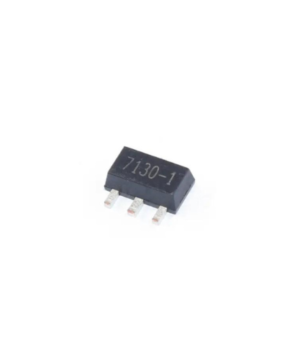
New original LDO IC Chip 7130-1 SOT89-3 Low Dropout Regulators HT7130-1
Active & Passive Component
Active & Passive Component
Controller

Reviews
There are no reviews yet.